Saturday, August 17, 2013

TDA8356

Description

The TDA8356 is a power circuit for use in 90° and 110° colour deflection systems for field frequencies of 50 to 120 Hz. The circuit provides a DC driven vertical deflection output circuit, operating as a highly efficient class G system.
The vertical driver circuit is a bridge configuration. The deflection coil is connected between the output amplifiers, which are driven in opposite phase. An external resistor (RM) connected in series with the deflection coil provides internal feedback information. The differential input circuit is voltage driven. The input circuit has been adapted to enable it to be used with the TDA9150, TDA9151B, TDA9160A, TDA9162, TDA8366 and TDA8376 which deliver symmetrical current signals. An external resistor (RCON) connected between the differential input determines the output current through the deflection coil.
The relationship between the differential input current and the output current is defined by: Idiff ´ RCON = Icoil ´ RM. The output current is adjustable from 0.5 A (p-p) to 2 A (p-p) by varying RM. The maximum input differential voltage is 1.8 V. In the application it is recommended that Vdiff = 1.5 V (typ). This is recommended because of the spread of input current and the spread in the value of RCON.
The flyback voltage is determined by an additional supply voltage VFB. The principle of operating with two supply voltages (class G) makes it possible to fix the supply voltage VP optimum for the scan voltage and the second supply voltage VFB optimum for the flyback voltage. Using this method, very high efficiency is achieved.

Download Datasheet TDA8356

Friday, July 5, 2013

REG1117

Description

The REG1117 is a family of easy-to-use three-terminal voltage regulators. The family includes a variety of fixed and adjustable-voltage versions, two currents (800mA and 1A) and two package types (SOT-223 and DDPAK). Output voltage of the adjustable versions is set with two external resistors. The REG1117 low dropout voltage allows its use with as little as 1V input-output voltage differential.
Laser trimming assures excellent output voltage accuracy without adjustment. An NPN output stage allows output stage drive to contribute to the load current for maximum
efficiency.

Features:
  • Fixed and Adjustable versions
  • 2.85V model for SCSI-2 active Termination
  • Output Current:
    REG1117: 800mA max
    REG1117A: 1A max
  • Output Tolerance:  1% max
  • Dropout Voltage:
    REG1117: 1.2V max at IO = 800mA
    REG1117A: 1.3V max at IO = 1A
  • Internal Current limit
  • Thermal overload Protection
  • SOT-223 and DDPAK Surface-mount packages
Applications:
  • SCSI-2 Active Termination
  • Hand-Held Data collection devices
  • High Efficiency Linear Regulators
  • Battery-Powered Instrumentation
  • Battery Management Circuits for Notebook and PALMTOP PCs
  • Core Voltage Supply: FPGA, PLD, DSP, CPU
Pinout Connection
Download Datasheet REG1117

Sunday, June 30, 2013

CD4066B

Description

The CD4066B is a quad bilateral switch intended for the transmission or multiplexing of analog or digital signals. It is pin-for-pin compatible with the CD4016B, but exhibits a much lower on-state resistance. In addition, the on-state resistance is relatively constant over the full signal-input range.
The CD4066B consists of four bilateral switches, each with independent controls. Both the p and the n devices in a given switch are biased on or off simultaneously by the control signal. This configuration eliminates the variation of the switch-transistor threshold voltage with input signal and, thus, keeps the on-state resistance low over the full operating-signal range.
The advantages over single-channel switches include peak input-signal voltage swings equal to the full supply voltage and more constant on-state impedance over the input-signal range. However, for sample-and-hold applications, the CD4016B is recommended.

Features:
  • 15-V Digital or ±7.5-V Peak-to-Peak Switching
  • 125-Ω Typical On-State Resistance for 15-V Operation
  • Switch On-State Resistance Matched to Within 5 Ω Over 15-V Signal-Input Range
  • On-State Resistance Flat Over Full Peak-to-Peak Signal Range
  • High On/Off Output-Voltage Ratio: 80 dB Typical at fis = 10 kHz, RL = 1 kΩ
  • High Degree of Linearity: <0.5% Distortion Typical at fis = 1 kHz, Vis = 5 V p-p, VDD − VSS ≥ 10 V, RL = 10 kΩ
  • Extremely Low Off-State Switch Leakage, Resulting in Very Low Offset Current and High Effective Off-State Resistance: 10 pA Typical at VDD − VSS = 10 V, TA = 25°C
  • Extremely High Control Input Impedance (Control Circuit Isolated From Signal Circuit): 1012 Ω Typical
  • Low Crosstalk Between Switches: −50 dB Typical at fis = 8 MHz, RL = 1 kΩ
  • Matched Control-Input to Signal-Output Capacitance: Reduces Output Signal Transients
  • Frequency Response, Switch On = 40 MHz Typical
  • 100% Tested for Quiescent Current at 20 V
  • 5-V, 10-V, and 15-V Parametric Ratings
  • Meets All Requirements of JEDEC Tentative Standard No. 13-B, Standard Specifications for Description of “B” Series CMOS Devices
Apllications:
  • Analog Signal Switching/Multiplexing: Signal Gating, Modulator, Squelch Control, Demodulator, Chopper, Commutating Switch
  • Digital Signal Switching/Multiplexing
  • Transmission-Gate Logic Implementation
  • Analog-to-Digital and Digital-to-Analog Conversion
  • Digital Control of Frequency, Impedance, Phase, and Analog-Signal Gain
Pinout CD4066

 Download Datasheet CD4066B

TLC072CP

 Description

The JFET-input operational amplifiers in the TL07_ series are designed as low-noise versions of the TL08_ series amplifiers with low input bias and offset currents and fast slew rate. The low harmonic distortion and low noise make the TL07_ series ideally suited for high-fidelity and audio preamplifier applications. Each amplifier features JFET inputs (for high input impedance) coupled with bipolar output stages integrated on a single monolithic chip.
The C-suffix devices are characterized for operation from 0°C to 70°C. The I-suffix devices are characterized for operation from –40°C to 85°C. The M-suffix devices are characterized for operation over the full military temperature range of –55°C to 125°C.

Features:
  • Low Power Consumption
  • Wide Common-Mode and Differential Voltage Ranges
  • Low Input Bias and Offset Currents
  • Output Short-Circuit Protection
  • Low Total Harmonic Distortion 0.003% Typ
  • Low Noise Vn = 18 nV//Hz Typ at f = 1 kHz
  • High Input Impedance . . . JFET Input Stage
  • Internal Frequency Compensation
  • Latch-Up-Free Operation
  • High Slew Rate . . . 13 V/ms Typ
  • Common-Mode Input Voltage Range Includes VCC+

Pin Connection
Download Datasheet TL072CP

Saturday, June 29, 2013

NE555


Desription


TheNE555monolithic timing circuit isa highlystable controller capableofproducingaccuratetime delays or oscillation. In the time delay mode of operation, the time is precisely controlled by one external resistor and capacitor. For astable operation as an oscillator, the free running frequency and the duty cycle are both accurately controlled with two external resistors and one capacitor. The circuit may be triggered and reset on falling waveforms, and the output structure can source or sink up to 200mA. The NE555 is available in plastic and ceramic mini dip package and in a 8-lead micro package and in metal can package version.

Features
  • Low turn OFF time
  • Maximum operating frequency greater han 500kHz
  • Timing from micro seconds to hours
  • Operates in both astable and monostable modes
  • High output current can source or sink 200mA
  • TTL Compatible
  • Temperature stability of 0.0005% PeroC
Pin Connection
 Download Datasheet NE555

Monday, June 17, 2013

ATMEGA64

Description

The ATmega64 is a low-power CMOS 8-bit microcontroller based on the AVR enhanced RISC architecture. By executing powerful instructions in a single clock cycle, the ATmega64 achieves throughputs approaching 1 MIPS per MHz, allowing the system designer to optimize power consumption versus processing speed.
The AVR core combines a rich instruction set with 32 general  purpose working registers. All the 32 registers are directly connected to the Arithmetic Logic Unit (ALU), allowing two independent registers to be accessed in one single instruction executed in one clock cycle. The resulting architecture is more code efficient while achieving throughputs up to ten times faster than conventional CISC microcontrollers.

The ATmega64 provides the following features: 64 Kbytes of In-System Programmable Flash with Read-While-Write capabilities, 2 Kbytes EEPROM, 4 Kbytes SRAM, 53 general purpose I/O lines, 32 general purpose working registers, Real Time Counter (RTC), four flexible Timer/Counters with compare modes and PWM, two USARTs, a byte oriented Two-wire Serial Interface, an 8-channel, 10-bit ADC with optional differential input stage with programmable gain, programmable Watchdog Timer with internal  Oscillator, an SPI serial port, IEEE std. 1149.1 compliant JTAG test interface, also used for accessing the On-chip Debug system and programming, and six software selectable power saving modes. The Idle mode stops the CPU while allowing the SRAM, Timer/Counters, SPI port, and interrupt system to continue functioning. The Power-down mode saves the register contents but freezes the Oscillator, disabling all other chip functions until the next interrupt or Hardware Reset. In Power-save mode, the asynchronous timer continues to run, allowing the user to maintain a timer base while the rest of the device is sleeping. The ADC Noise Reduction mode stops the CPU and all I/O modules except asynchronous timer and ADC, to minimize switching noise during ADC conversions. In Standby mode, the crystal/resonator Oscillator is running while the rest of the device is sleeping. This allows very fast start-up combined with low power consumption. In Extended Standby mode, both the main Oscillator and the asynchronous timer continue to run.

Pinout ATMEGA64
Download Datasheet ATMEGA64

Sunday, June 16, 2013

AT89C51

Description

 The AT89C51 is a low-power, high-performance CMOS 8-bit microcomputer with 4Kbytes of Flash programmable and erasable read only memory (PEROM). The device is manufactured using Atmel’s high-density nonvolatile memory technology and is compatible with the industry-standard MCS-51 instruction set and pinout. The on-chip Flash allows the program memory to be reprogrammed in-system or by a conventional nonvolatile memory programmer. By combining a versatile 8-bit CPU with Flash on a monolithic chip, the Atmel AT89C51 is a powerful microcomputer which provides a highly-flexible and cost-effective solution to many embedded control applications.

The AT89C51 provides the following standard features: 4K bytes of Flash, 128 bytes of RAM, 32 I/O lines, two 16-bit timer/counters, a five vector two-level interrupt architecture, a full duplex serial port, on-chip oscillator and clock circuitry. In addition, the AT89C51 is designed with static logic for operation down to zero frequency and supports two software selectable power saving modes. The Idle Mode stops the CPU while allowing the RAM, timer/counters, serial port and interrupt system to continue functioning. The Power-down Mode saves the RAM contents but freezes the oscillator disabling all other chip functions until the next hardware reset.


Features
  • Compatible with MCS-51™ Products
  • 4K Bytes of In-System Reprogrammable Flash Memory
  • Fully Static Operation: 0 Hz to 24 MHz
  • Three-level Program Memory Lock
  • 128 x 8-bit Internal RAM
  • 32 Programmable I/O Lines
  • Two 16-bit Timer/Counters
  • Six Interrupt Sources
  • Programmable Serial Channel
  • Low-power Idle and Power-down Modes
Pinout Diagram


Download Datasheet AT89C51

Sunday, April 21, 2013

LM2576

Description

The LM2576 series of regulators are monolithic integrated circuits that provide all the active functions for a step-down (buck) switching regulator, capable of driving 3A load with excellent line and load regulation. These devices are available in fixed output voltages of 3.3V, 5V, 12V, 15V, and an adjustable output version. Requiring a minimum number of external components, these regulators are simple to use and include internal frequency compensation and a fixed frequency oscillator.

The LM2576 series offers a high-efficiency replacement for popular three-terminal linear regulators. It substantially reduces the size of the heat sink, and in some cases no heat sink is required. A standard series of inductors optimized for use with the LM2576 are available from several different manufacturers. This feature greatly simplifies the design of switch-mode power supplies. Other features include a specified ±4% tolerance on output voltage within specified input voltages and output load conditions, and ±10% on the oscillator frequency. External shutdown is included, featuring 50μA (typical) standby current. The output switch includes cycle-by-cycle current limiting, as well as thermal shutdown for full protection under fault conditions.

Blok Diagram
Download Datasheet LM2576

TDA2030

DESCRIPTION

The TDA2030 is a monolithic integrated circuit in Penta watt® package, intended for use as a low frequency class AB amplifier. Typically it provides 14W output power (d = 0.5%) at 14V/4Ω; at ± 14V or 28V, the guaranteed output power is 12W on a 4Ω load and 8W on a 8Ω (DIN45500).

The TDA2030 provides high output current and has very low harmonic and cross-over distortion. Further the device incorporates an original (and patented) short circuit protection system comprising an arrangement for automatically limiting the dissipated power so as to keep the working point of the output transistors within their safe operating area. A conventional thermal shut-down system is also included.

PRACTICAL CONSIDERATIONS

Printed circuit board
The layout shown in Fig. 1 should be adopted by the designers. If different layouts are used, the
ground points of input 1 and input 2 must be well decoupled from the ground return of the output in
which a high current flows.
 Fig 1

Assembly suggestion
No electrical isolation is needed between the package and the heatsink with single supply voltage configuration.


Application suggestions
The recommended values of the components are those shown on application circuit of fig. 2. Different values can be used. The following table can help the designer.

Fig 2
SHORT CIRCUIT PROTECTION
The TDA2030 has an original circuit which limits the current of the output transistors. Fig. 3 shows that the maximum output current is a function of the collector emitter voltage; hence the output transistors work within their safe operating area. This function can therefore be considered as being peak power limiting rather than simple current limiting. It reduces the possibility that the device gets damaged during an accidental short circuit from AC output to ground.
 Fig 3
THERMAL SHUT-DOWN
The presence of a thermal limiting circuit offers the following advantages:
  1. An overload on the output (even if it is permanent), or an above limit ambient temperature can be easily supported since the Tj cannot be higher than 150°C.
  2. The heatsink can have a smaller factor of safety compared with that of a conventional circuit. There is no possibility of device damage due to high junction temperature. If for any reason, the junction temperature increases up to 150°C, the thermal shut-down simply reduces the power dissipation at the current consumption.
The maximum allowable power dissipation depends upon the size of the external heatsink (i.e. its
thermal resistance).

AT90S2313


Description


The AT90S2313 is a low-power CMOS 8-bit microcontroller based on the AVR RISC architecture. By executing powerful instructions in a single clock cycle, the AT90S2313 achieves throughputs approaching 1 MIPS per MHz allowing the system designer to optimize power consumption versus processing speed.

The AVR core combines a rich instruction set with 32 general purpose working registers. All the 32 registers are directly connected to the Arithmetic Logic Unit (ALU), allowing two independent registers to be accessed in one single instruction executed in one clock cycle. The resulting architecture is more code efficient while achieving through puts up to ten times faster than conventional CISC micro controllers.

The AT90S2313 provides the following features: 2K bytes of In-System Programmable Flash, 128bytes EEPROM, 128 bytes SRAM, 15 general purpose I/O lines, 32 general purpose working registers, flexible Timer/Counters with compare modes, internal and external interrupts, a programmable serial UART, programmable Watchdog Timer with internal Oscillator, an SPI serial port for Flash memory downloading and two software selectable power-saving modes. The Idle mode stops the CPU while allowing the SRAM, Timer/Counters, SPI port and interrupt system to continue functioning. The Power-down mode saves the register contents but freezes the Oscillator, disabling all other chip functions until the next external interrupt or Hardware Reset.

The device is manufactured using Atmel’s high-density non-volatile memory technology. The On-chip In-System Programmable Flash allows the Program memory to be reprogrammed in-system through an SPI serial interface or by a conventional non-volatile memory programmer. By combining an enhanced RISC 8-bit CPU with In-System Programmable Flash on a monolithic chip, the Atmel AT90S2313 is a powerful microcontroller that provides a highly flexible and cost-effective solution to many embedded control applications.

The AT90S2313 AVR is supported with a full suite of program and system development tools including: C compilers, macro assemblers, program debugger/simulators, In-Circuit Emulators and evaluation kits.

Features
  • Utilizes the AVR ® RISC Architecture
  • AVR High Performance and Low Power RISC Architecture
  • 118 Powerful Instructions
  • Most Single Clock Cycle Execution
  • 32 x 8 General Purpose Working Registers
  • Up to 10 MIPS Throughput at 10 MHz
  •  Data and Non-volatile Program Memory
  • 2K Bytes of In-System Programmable Flash Endurance 1,000 Write/Erase Cycles
  • 128 Bytes of SRAM
  • 128 Bytes of In-System Programmable EEPROM Endurance: 100,000 Write/Erase Cycles
  • Programming Lock for Flash Program and EEPROM Data Security
  •  Peripheral Features
  • One 8-bit Timer/Counter with Separate Prescaler 
  • One 16-bit Timer/Counter with Separate Prescaler, Compare, Capture Modes and 8, 9, or 10 bit PWM
  • On-chip Analog Comparator
  • Programmable Watchdog Timer with On-chip Oscillator
  • SPI Serial Interface for In-System Programming 
  • Full Duplex UART
  • Special Micro controller Features
  • Low Power Idle and Power-down Modes
  • External and Internal Interrupt Sources
  • Specifications
  • Low-power, High-speed CMOS Process Technology
  • Fully Static Operation
  • Power Consumption at 4 MHz, 3V, 25°C
  • Active: 2.8 mA
  • Idle Mode: 0.8 mA
  • Power-down Mode: <1 µA
  •  I/O and Packages
  • 15 Programmable I/O Lines
  • 20-pin PDIP and SOIC
  • Operating Voltages
  • 2.7 - 6.0V (AT90S2313-4)
  • 4.0 - 6.0V (AT90S2313-10)
  • Speed Grades
  • 0 - 4 MHz (AT90S2313-4)
  • 0 - 10 MHz (AT90S2313-10)
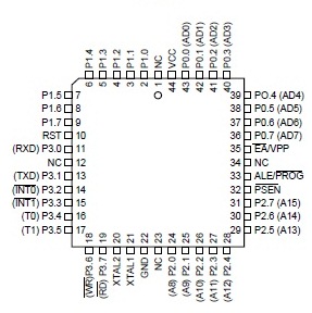
 Pin Configuration

Download Datasheet AT90S2313

Sunday, April 7, 2013

LM358

Description

The LM2904,LM358/LM358A, LM258/LM258A consist of two independent, high gain, internally frequency compensated operational amplifiers which were designed specifically to operate from a single power supply over a wide range of voltage. Operation from split power supplies is also possible and the low power supply current drain is independent of the magnitude of the power supply voltage. Application areas include transducer amplifier, DC gain blocks and all the conventional OP-AMP circuits which now can be easily implemented in single power supply systems.

Internal Blok Diagram
Schematic Diagram
Download Datasheet LM358

TDA2009A

Description

The TDA2009A is class AB dual Hi-Fi Audio power amplifier assembled in Multi watt Ò package, specially designed for high quality stereo application as Hi-Fi and music centers.

Build-In Protection Systems

Tehrmal Shut-DOwn
The presence of a thermal limiting circuit offers the following advantages:
  1. an averload on the output (even if it is permanent), or an excessive ambient temperature can be easily withstood.
  2. the heatsink can have a smaller factor of safety compared with that of a conventional circuit. There is no device damage in the case of excessive junction temperature : all that happens is that Po (and therefore Ptot) and Io are reduced.
The maximum allowable power dissipation depends upon the size of the external heatsink (i.e.its thermal resistance); Short circuit (AC Conditions). The TDA2009A can withstand an accidental short circuit from the output and ground made by a wrong connection during normal play operation.

Mounting Intructions
The power dissipated in the circuit must be removed by adding an external heatsink. Thanks to the MULTIWATT Ò package attaching the heatsink is very simple, a screw or a compression spring  (clip) being sufficient. Between the heatsink and the package it is better to insert a layer of silicon grease, to optimize the thermal contact,  no electrical isolation is needed between the two


Download Dataseheet TDA2009A

Friday, March 8, 2013

TDA2006

Description

The TDA2006 is a monolithic integrated circuit in Pent a watt package, intended for use as a low frequency class”AB” amplifier. At ±12V,d = 10 % typically it provides12W output power on a 4Ω load and 8W on a 8Ω . The TDA2006 provides high output current and has very low harmonic and cross-over distortion. Further the device incorporates an original (and  patented) short circuit protection system comprising an arrangement for automatically limiting the dissipated power so as to keep the working point of the output transistors within their safe operating area. A conventional thermal shutdown system is also included. The TDA2006 is pin to pin equivalent to theTDA2030.

Pin Connection


 PRACTICALCONSIDERATIONS

Printed Circuit Board


The layout shown in Figure should be adopted by the designers. If different layout are used, the ground points of input 1 and input 2 must be well decoupled from ground of the output on which a
rather high current flows.

Assembly Suggestion

No electrical isolation is needed between the package and the heat-sink with single supply voltage
configuration.

Application Suggestion

The recommended values of the components are the ones show non application circuits of Figure Above. Different values can be used.The table1 can help the designers.
Table 1 :


Download Datasheet TDA2006

TA8248K

Low Frequency Power Amplifier


TA8248K is an audio power IC with built-in two channels developed for portable radio cassette tape recorder with power ON/OFF switch. Because of the parts reduction and SIP (Single Inline Package),space merit is remarkable. Thermal shut down protection circuit is built in.

Features :
  • High Power
         Pout (1) = 2.5 W (typ.)
         (VCC = 9 V, RL = 4Ω, f = 1 kHz, THD = 10%)
         Pout (2) = 4.6 W (typ.)
         (VCC = 12 V, RL = 4Ω, f = 1 kHz, THD = 10%)
  • Low Popping Noise at Power ON
  • Small Quiescent Current
    ICCQ = 21 mA (typ.) (VCC = 15 V, Vin = 0)
  • Soft Clip
  • Built-in Thermal Shut Down Protection Circuit
  • Best for Supply Voltage 9 V, 12 V
  • Operation Supply Voltage Range : VCC (opr) = 6~15 V (Ta = 25°C)


Blok Diagram


Application Information And Application Method

  1. Adjustment of voltage gain
The voltage gain Gv is obtained as follows by R1, R2 and Rf in Fig.1.
 Figure 1


By increasing Rf, reduction of Gv is possible. However, since the feedback increase is liable to produce oscillation, it is recommended to use this at 40dB or over.

Thermal shut-down circuit
The thermal shut-down circuit is built in for the purpose of preventing the destruction of IC due to the
abnormal temperature rise when the heat radiation is insufficient. The operation temperature is set at radiation Fin temperature 175°C (typ.). At this temperature or over the bias is interrupted to prevent the destruction of IC.

Download Datasheet TA8428K